


The Application Prospect of Inkjet Printing Technology in PCB Manufacturing and a Detailed Explanation of Single-sided Board UV Ink Process
Abstract:
This paper first explores the application advantages and development prospects of digital inkjet printing technology in printed circuit board (PCB) manufacturing. It then focuses on analyzing three key UV inks used in traditional single-sided board manufacturing processes: UV anti-etching ink, UV solder mask ink, and UV character ink, with detailed descriptions of their application scenarios, performance requirements, and main component compositions. The paper provides a technical reference for understanding the development of PCB manufacturing processes.
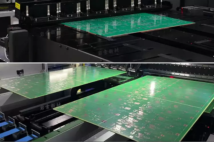
As the core carrier for component mounting and electrical connection in modern electronic devices, printed circuit boards (PCB) are indispensable basic components in the electronics industry. With the rapid development of electronic technology, especially the breakthrough progress in digital inkjet printing technology, PCB manufacturing processes are undergoing a revolutionary transformation.
Digital inkjet printing technology significantly optimizes the traditional PCB manufacturing process by directly and precisely jet-printing conductive circuits, solder mask inks, and character inks on the substrate. This technology boasts the following prominent advantages:
✿ 1. Greatly shortening the production cycle
✿ 2. Enabling higher-precision miniaturization
✿ 3. Significantly reducing production costs
✿ 4. Being more environmentally friendly
✿ 5. Being applicable to the manufacturing of inner layers of multi-layer boards
With the continuous innovation and technological maturity of inkjet printing technology, the "all-printed electronics" technology is expected to be widely applied in the PCB industry. However, the current mainstream PCB manufacturing still mainly relies on traditional printing methods, including screen printing, dry film, and wet film processes, among others.
一、Analysis of Single-sided Board Manufacturing Process
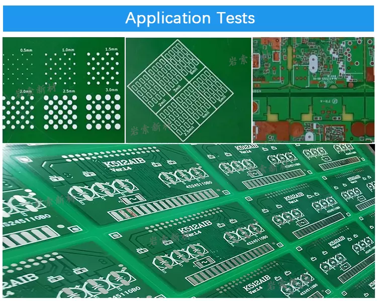
According to the number of circuit layers, PCBs can be divided into single-sided boards, double-sided boards, multi-layer boards and build-up multi-layer boards, each with distinct characteristics in terms of manufacturing processes and material selection. Currently, mainstream processes generally adopt photo-curing materials, such as UV inks, dry films, photoimageable inks and point-deposited photoresists.
As a basic PCB product, the typical manufacturing process of single-sided boards is as follows:
✿ 1. Pretreatment of copper-clad laminates
✿ 2. Screen printing of UV anti-etching ink
✿ 3. UV curing
✿ 4. Etching (selective electroplating)
✿ 5. Film stripping and drying
✿ 6. Screen printing of UV solder mask ink
✿ 7. UV curing
✿ 8. Screen printing of UV character ink
✿ 9. UV curing
✿ 10. Final inspection
This process requires three key types of UV inks: anti-etching ink, solder mask ink, and character ink. The technical characteristics of these three inks will be introduced in detail below.
二、 Analysis of Three Key UV Ink Technologies
1.1 UV Anti-etching Ink Technology
In PCB manufacturing, copper circuits are formed by chemically etching the copper foil on copper-clad laminates. UV anti-etching ink functions to protect the circuit parts that do not need to be etched, and must meet the following technical requirements:
✿ 1. Excellent adhesion to copper foil
✿ 2. Corrosion resistance and electroplating performance
✿ 3. Good solubility in 3% sodium hydroxide solution (for easy removal)
1.2 Typical formulation of UV anti-etching ink
✿ 1. Alkali-soluble photosensitive resin system (such as anhydride-modified epoxy acrylate resin, high acid value polyester acrylate resin, or modified maleic anhydride resin, etc.)
✿ 2. Acrylate functional monomer
✿ 3. Photoinitiator (651 or 2-ethylanthraquinone)
✿ 4. Colorant (approximately 1% phthalocyanine blue)
✿ 5. Filler (talc powder, fumed silica, etc.)
✿ 6. Carboxyl-containing alkali-soluble resin
2.1 UV Solder Mask Ink Technology
As a permanent protective layer for PCBs, the main functions of solder mask ink include:
✿ 1. Preventing improper adhesion of solder
✿ 2. Enhancing electrical insulation performance
✿ 3. Withstanding high-temperature soldering
✿ 4. Resisting moisture, mildew, and oxidation
2.2 Typical Formulation of UV Solder Mask Ink
✿ 1. Resin base (such as bisphenol A epoxy acrylate resin, novolac epoxy acrylate resin, and polyurethane acrylate resin, etc.)
✿ 2. Multifunctional acrylates combined with monofunctional (meth)acrylic hydroxyl esters (conducive to the ink's adhesion to copper)
✿ 3. Photoinitiator (651 or 2-ethylanthraquinone)
✿ 4. Colorant (<1% phthalocyanine green)
✿ 5. A relatively large amount of fillers
✿ 6. 1-2% of adhesion promoters (methacrylic acid phosphonate), defoamers, leveling agents, polymerization inhibitors, etc.
3.1 UV Character Ink Technology
Character ink is used for marking printing on PCBs, with the main requirements including:
✿ 1. Excellent recognizability
✿ 2. Good weather resistance
✿ 3. High-temperature solder resistance comparable to that of solder mask ink
3.2 Typical formulation of UV character ink
✿ 1. Bisphenol A epoxy acrylate resin, novolac epoxy acrylate resin, polyurethane acrylate resin, etc.
✿ 2. Titanium dioxide and other high hiding pigments
✿ 3. Photoinitiators ( TPO、184、MBF、819、784、369、907、ITX、DETX )
✿ 4. Rheology modifiers (fumed silica)
This paper details the key UV ink technologies used in the manufacturing of single-sided boards. In subsequent articles, we will continue to explore the manufacturing processes and material technology developments of more complex PCB products such as double-sided boards and multi-layer boards. As electronic devices move toward higher performance and miniaturization, PCB manufacturing technology will continue to innovate, providing solid support for the development of the electronics industry.
If you have any product requirements or technical inquiries, please feel free to contact us at any time. We look forward to cooperating with you!